Digital Potentiometers (DP) represent a modern alternative to the traditional mechanical versions, although both still have their particular fields of application where one type exceeds the other in terms of efficiency, precision or reliability. When working with microcontrollers, every time the program requires changing an external variable, such as an amplifier’s gain or the voltage of a variable power supply, DPs appear as the component of choice, over the mechanical counterparts. The reason for this preference is simple: a DP accepts a digital value and converts it into a proportional resistance value; no mechanical parts, such as motors or servomechanisms, are involved. The widespread usage of these components has increased their availability and reduced the price, so they are an ideal companion for any microcontroller project that requires changing an analog variable. We will review how to use them with PIC Microcontrollers, the practical implications and the real life behavior.
A DP can be seen as a black box, with inputs and outputs. On the inputs side, it will accept digital commands and data from a microcontroller; on the outputs side, it will behave as a three-terminal potentiometer, with the two extremes of the resistor and the moving wiper available to the user. The position of the wiper is controlled by the digital data. Figure 1 shows a simplified diagram of a DP.
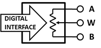 FIGURE 1.- Digital Potentiometer
Between A and B the maximum value of the potentiometer will be read, while the values A-W and B-W depend on the data being received through the digital interface. This interface can be one of several protocols; for this analysis we will be using DPs with SPI interface, since it is simple, widely used, and can be easily simulated by software, in case the selected microcontroller does not have it implemented in its hardware.
A typical SPI connection is shown in Figure 2.
 FIGURE 2.- SPI Master-Slave connection
The first three lines, CLOCK, MOSI and MISO, are the SPI bus, while CHIP SELECT is used to identify the target device. In this configuration, the microcontroller is the Master, while the DP is the Slave; the direction of the arrows indicates this arrangement. MOSI means “Master Out, Slave In”, while MISO is “Master In, Slave Out”. As shown, the SPI protocol permits a bi-directional data flow, although we will not be using the MISO line in this tutorial.
Practical implementation
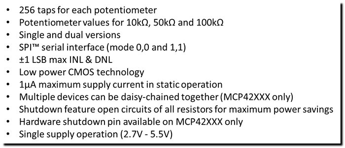
The DPs we will be using belong to the MCP41XXX/42XXX series by Microchip. A brief description of their characteristics, as found in the datasheet:
In the first example we will be using the MCP41010, i.e. the single version of the 10kΩ DP. The test setup is shown in Figure 3.
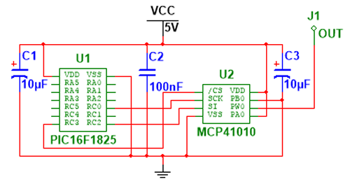 FIGURE 3.-Schematic diagram using a single version DP
The B terminal of the DP (PB0) is connected to ground; the reason for this is that the wiper goes to this terminal when the data is 0, and moves towards A (PA0) as the value increases. In this sense, the voltage value seen in the wiper terminal is directly proportional to the digital data, since A is tied to the supply voltage.
The microcontroller is the PIC16F1825, which has SPI implemented by hardware. SCK corresponds to PIN C0 (RC0), SDO is PIN C2 (RC2) and SDI is PIN C1 (RC1). This last terminal is left open, as it will not be used (already explained). The CHIP SELECT function will be performed by PIN C3 (RC3). Since we will be using the internal clock of the microcontroller, there is no need to add any external crystal, so the only other connection required is the power supply. The capacitors, 10µF tantalum, are mounted as close as possible to the power supply pins in each chip; together with the 0.1µF ceramic mounted on the power line, their function is to reduce the electrical noise created by the digital transitions. This topic will be further analyzed later.
With this setup, and the proper program running, the wiper of the DP may go from 0V to 5V, or any of the various values between these extremes, a total of 256 steps.
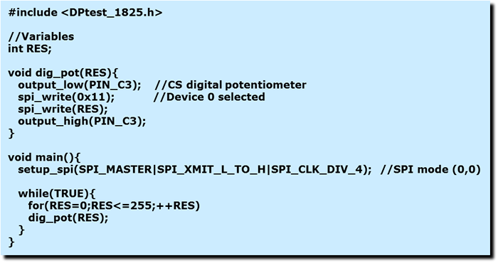
An interesting test is to send these 256 values sequentially, and repeat the routine indefinitely. In this way, the variation of the wiper, thus the analog voltage, can be easily seen in an oscilloscope. Here is a very simple program to do this (programmed using CCS C).
 (
(The PIC16F1825 configuration file is listed below.
 (
(The concept is simple: an 8-bit variable (int) named RES is loaded sequentially from 0 to 255 [in the for(;;) loop]. Every time a new value is loaded, the DP writing routine is called [dig_pot(RES)], and the contents of RES are sent to the DP. Once 255 is reached, the cycle starts all over again, indefinitely [while(TRUE)]. And that’s all; the only other line required in the main program is the SPI setup, the PIC configured as Master, in mode 0,0 (the SCK idles at 0V) and using the internal clock divided by 4.
Let’s now look at the DP writing routine [dig_pot(RES)], which is the most relevant part of this article. The first thing to do is call the target chip; therefore, the CS line (PIN_C3) goes to a low state. After this, the actual writing of the DP occurs [spi_write()]; two values are sent: 0x11, and RES. As we already know that RES contains the value we would like to write in the DP to move the wiper, the other value (0x11) must be a sort of command. As a matter of fact, it is; the DP requires a command to be sent first, and then the actual data.
What information is transmitted in this command? The DP datasheet explains it.
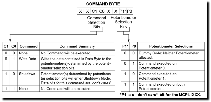
The upper nibble of the command byte indicates the action to be performed; the lower nibble, in which of the DPs it will be executed. This command byte is common to the single and dual versions, so all references to P1 (the second DP) are only valid for the dual version, MCP42XXX. In our example, only P0 is available. Later on we will work with the dual version, to show how to write to each DP.
It should be now clear that the command 0x11 (0001 0001) indicates “Write Data” on “Potentiometer 0”. So the contents of RES are effectively written on DP0 and the wiper is moved accordingly. This last action only occurs after the CS line is brought back to a high state, which is the final sentence of the routine.
Once the program is running, the wiper will show sequentially the voltage of each of the 256 steps, starting at 0V. Figure 4 shows the actual waveform as seen on an oscilloscope.
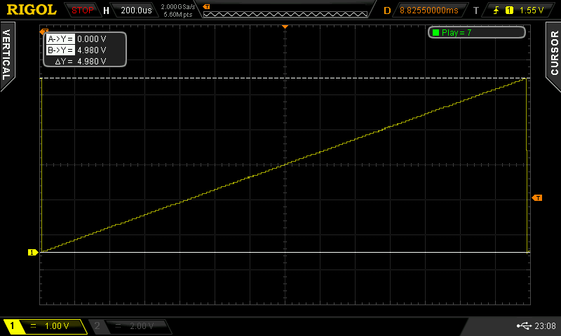
FIGURE 4.- Full voltage swing at the DP output, from 0V to 4.98V
The steps are clearly seen, moving from 0V to 4.98V. Why not 5V? The answer is simple: the output voltage is calculated as:

Given that Vmax is 5V, D_value is an 8-bit variable (RES) and there are 256 steps, the maximum value of Vout (when RES is 255) will be:
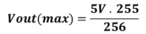
Which gives approximately 4.98V. Is it possible to get the full 5V? Yes, but not with this family of DPs. There are other families with 257 steps; the additional step (1 bit sent in the command byte) effectively connects the wiper with the A terminal, having the full swing from 0V to 5V. For more information please refer to the MCP415X/425X family.
What if the desired voltage swing is different from the full supply voltage, let’s say a reduced variation in order to feed an amplifier connected to the same supply, without saturating the inputs? The DP behaves as an analog resistor, so it can be a part of a standard voltage divider, as shown in Figure 5.
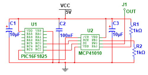 FIGURE 5.- DP connected as part of a voltage divider
R1, DP and R2 form a voltage divider. The total resistance is 12kΩ, since DP is 10kΩ and each discrete resistor is 1kΩ. Therefore the current is 5V/12kΩ, i.e. 0.417mA. The voltage swing in the DP goes now from 0.417V (1kΩ x 0.417mA) to 4.583V (11kΩ x 0.417mA). This voltage can now be used to drive an amplifier (e.g. an Operational Amplifier) connected to the same power supply (5V) with no risk of saturating the inputs.
Step size and digital noise
We previously connected the DP directly to the power supply (5V), and mentioned that there are 256 possible steps for the wiper to be located. What is the voltage difference between two consecutive steps, in other words, the step size? This is a simple calculation, 5V/256 steps gives a step size of approximately 19.5mV. What about the voltage divider? In this case the total voltage swing is 4.583V – 0.417V, i.e. 4.166V. Therefore, the step size is 4.166V/256 steps, equal to approximately 16.3mV.
We would like to confirm that the step size of the voltage divider is about 16mV, so we simply connect the output to the oscilloscope and zoom-in to see a transition, as shown in Figure 6.

FIGURE 6.- Steps seen at maximum resolution (5mV/div), with the circuit mounted on a breadboard; the digital noise is evident
This is probably something not expected, and that may discourage everyone that was considering using a DP for a precise voltage adjustment: the electrical noise introduced by the digital transitions moves though the power lines and reaches the output. This is something very common when using digital and analog circuits together, and can be a headache when it is not properly acknowledged. Can this be solved in any way? The answer is definitely yes.
To prove this point, please note that I mounted the previous test circuit in a breadboard, which is something everybody does when testing an initial concept. What is being shown is the result of the poor noise reduction you can achieve in a breadboard, particularly when mixing analog and digital signals.
Now, the same circuit mounted on a double-layer PCB, with ground planes on both sides, connected by several vias. The digital and analog traces are kept separated as much as possible. The result is shown in Figure 7.

FIGURE 7.- When the circuit is mounted on a double sided PCB with a ground plane, the signal appears clean (5mV/div)
The digital noise is completely gone. The signal is clean, and can be effectively used for precision adjustments. Additionally, we verified that the step size is around 16mV, as calculated.
Reducing the step size
In the previously shown examples, the step size was between 16 and 20mV. It is possible to reduce even further this value, provided the total voltage swing is reduced. For example, with a maximum voltage of 1V, the step size would be 3.9mV. What if we need to have an even smaller step but keeping a large voltage swing? One possibility would be to use a DP with more steps, if available. Another possibility is using the dual DP version, in an arrangement in which each DP contributes differently to the output voltage.
Before continuing, let’s analyze the circuit in Figure 8.
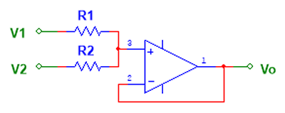 FIGURE 8.- Non-inverting summing circuit
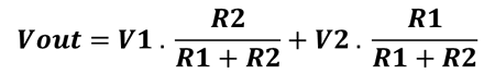
This is a non-inverting summing circuit, made with an operational amplifier. The transfer equation for this circuit is:
The output is the sum of the input voltages, V1 and V2, weighted by the series resistors, R1 and R2. Let’s consider the scenario where R1 is 100 times smaller than R2; then V1 will have 100 times more impact on Vout. Now, let’s assume that V1 and V2 are the outputs of two DPs, DP0 and DP1, respectively (to maintain the same names as in the DP’s datasheet). The step size of DP1 will be 100 times smaller than DP0, so we effectively reduced the step size, maintaining a large voltage swing. By properly designing the software, this “fine control” can be obtained over the whole scale.
Figure 9 shows a practical implementation of this concept.
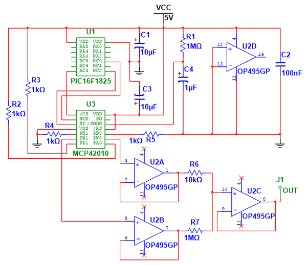 FIGURE 9.- Reduced step size using dual DP
Here, the dual DP, 10kΩ version is used. Both DPs are tied to 5V and 0V by 1kΩ resistors, so the voltage swing is limited, in order not to saturate the amplifier inputs. Each wiper is connected to a voltage follower, to isolate the DP from the summing circuit. DP0 voltage is connected by a 10kΩ resistor (R6), while DP1 by a 1MΩ resistor (R7). With this configuration, DP1 step should be 100 times smaller than DP0. Before we calculated that DP0 step was 16.3mV, so we should expect a resolution of 0.16mV from DP1.
There are a couple of new terminals in this DP chip, one of them is the reset (/RS), which is self-explanatory, and the other is the “shutdown” (/SHDN). This pin is connected to an RC circuit, to guarantee that the DP starts at 0 (wiper connected to B), and remains in this position for a while, until the microcontroller gains control of the wiper’s position. The time the DP remains at 0 depends on the RC time constant (1 second in this case); the program should guarantee that the microcontroller sends the proper command and data to the DP before the shutdown is released. If this precaution is not taken, the DP will always start with the wiper at the mid-point, which may result undesirable in some applications (e.g. when controlling a variable power supply).
Having explained the connection of the shutdown pin, let’s review the program to control de dual DP version, and how to implement this smaller step capability.
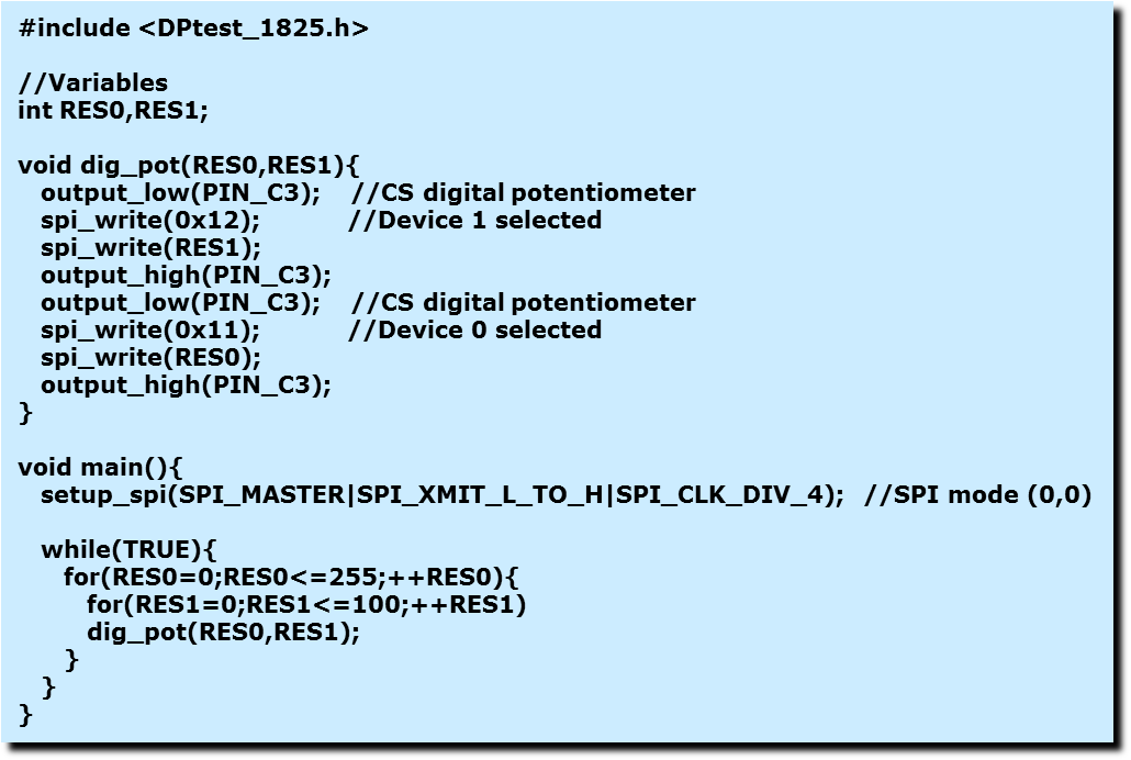 (
(The dig_pot routine now accepts two variables, RES0 and RES1, to control DP0 and DP1 respectively. The command byte now addresses each one of the DPs, and CS must be lowered and raised each time one of the DPs is written.
Inside the main program there is a double for(;;) loop; the internal moving DP1 100 steps, for every step DP0 is moved by the external loop.
Figure 10 shows how the voltage is seen at the output, at the oscilloscope's highest resolution (5mV/div).

FIGURE 10.- Reduced step size enables very fine control of the output voltage
A finer control has been achieved, and only using DPs with 256 steps. When reaching this level of precision, the remaining noise in the signal may be an issue, depending on the target application. Further noise reduction is possible, and feasible for most applications that need a constant level at the output, once the fine adjustment has been done, or at least a slow variation is the only requirement. Additional noise filtering may be applicable, leaving a clean DC voltage.
A final note on these DPs: the wiper can handle a maximum current of 1mA. Please exercise precaution when designing your particular application in order not to exceed this value.